Creating your own PCB seems to be an unavoidable task for every electronic enthusiast. Even when you plan to use a professional service to create the final PCB for your project, developing the skills to create your own PCB for prototypes and small projects will save you money and give you quick gratification. To assist with the PCB creation process I wanted a relative inexpensive digital microscope to inspect PCBs and solder joints. I had a $100 dollar budget. Over a couple of nights I researched available microscopes within my budget. I must say I was most impressed with the Dino-Lite family of products, unfortunately the cost of these units was outside of my budget. At the end of my research I settled for the Veho VMS-0004 Discovery. This post documents my first impressions of the Veho VMS-0004 microscope in the context of PCB design.
Installation
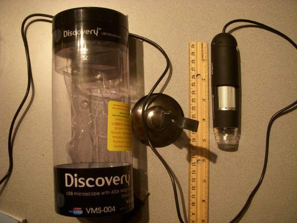
I picked a Veho Discovery from J&R in New York City for $69.99 + taxes. The unit comes in a slick cylindrical package. It comes with drivers for the MAC and PC. Unfortunately the CD is a small format and did not fit in my iMac. I had to use my laptop to transfer the content of the CD to a USB thumb drive in order to proceed with the installation. I installed the software in the Windows 7 64 bit partition of my iMac without any problems. Figure 1 contains a picture of the Veho and its base.
Test Run
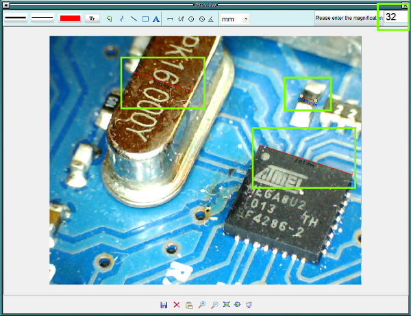
The Veho software let’s you take pictures and videos at high resolution. It also lets you measure objects as long as you provide the magnification from the microscope. I had mixed results with this feature. Figure 2 contains a picture of the MEGA82U micro controller and crystal in an Arduino Uno board at a 32x magnification. I have boxed in green the different measurements I took on the Arduino Uno. You will need to play with the magnification factor in order to get decent measurements.
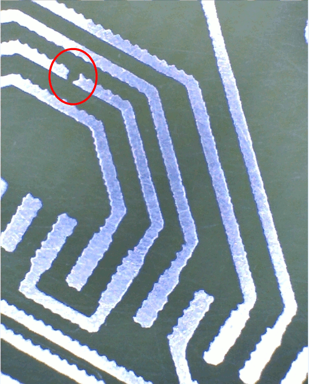
Figure 3 contains a picture of a broken trace in a PCB. The magnification of this picture is 30x. The broken trace is very difficult to see with the naked eye.
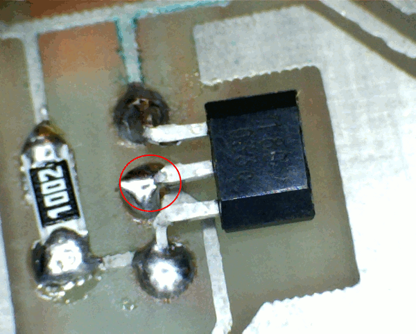
Figure 4 shows a hall effect sensor and a SMD resistor. The area in red shows a solder joint that needs additional work. The magnification for this picture is 30X.
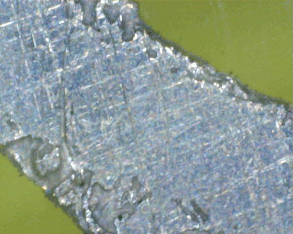
Figure 5 shows a portion of a trace magnified at 400x. You can see imperfections impossible to see with the naked eye.
The following video contains a few shot of a different PCBs. Hopefully you can see the level of magnification you can achieve with the Veho.
Conclusion
The Veho is made of hard plastic. The base is very light and tips over if the microscope is pushed too much forward. I am considering making a more robust base using PVC. The image quality is very good and the unit does a good job providing light to the area under inspection. For $69.99 + taxes, the Veho Discovery is a nice addition to your electronic workbench.

